
The Graphene Substrate Powering Photonic Computing
High-Performance Graphene Substrates for Femtosecond Optical Switching
THE PROBLEM
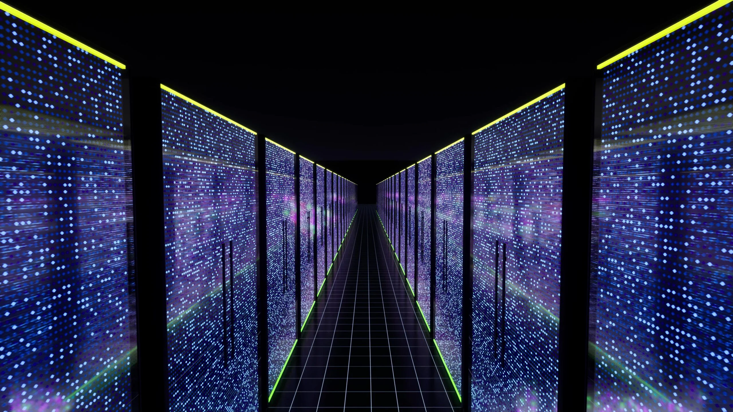
Computing Infrastructure Has Reached a Physical Limit
The growth of AI is exposing the limits of today’s computing infrastructure. As electronic systems work harder, they create more heat, require more power, and become more difficult and expensive to scale, creating a critical bottleneck.
This challenge is driving interest in optical computing, where information is processed using light rather than electrons. Photonic computing may provide the breakthrough by dramatically improving speed and efficiency.
Astera is building the graphene substrate platform that enables the next generation of photonic chips and is intended to make ultrafast photonic switching commercially possible
THE SOLUTION
Building the Critical Layer Behind Photonic Computing
Photonic computing represents the next major leap in performance, and Astera provides the materials that make it possible.
Astera is building an essential component through a graphene substrate engineered to support ultrafast photonic switching to help bridge the gap between technical promise and commercial deployment.
This positions Astera at a potentially valuable point in the value chain. Instead of competing at the crowded application level, the company is focused on the foundational material layer that could help enable the entire market.
ASTERA’S TECHNOLOGY
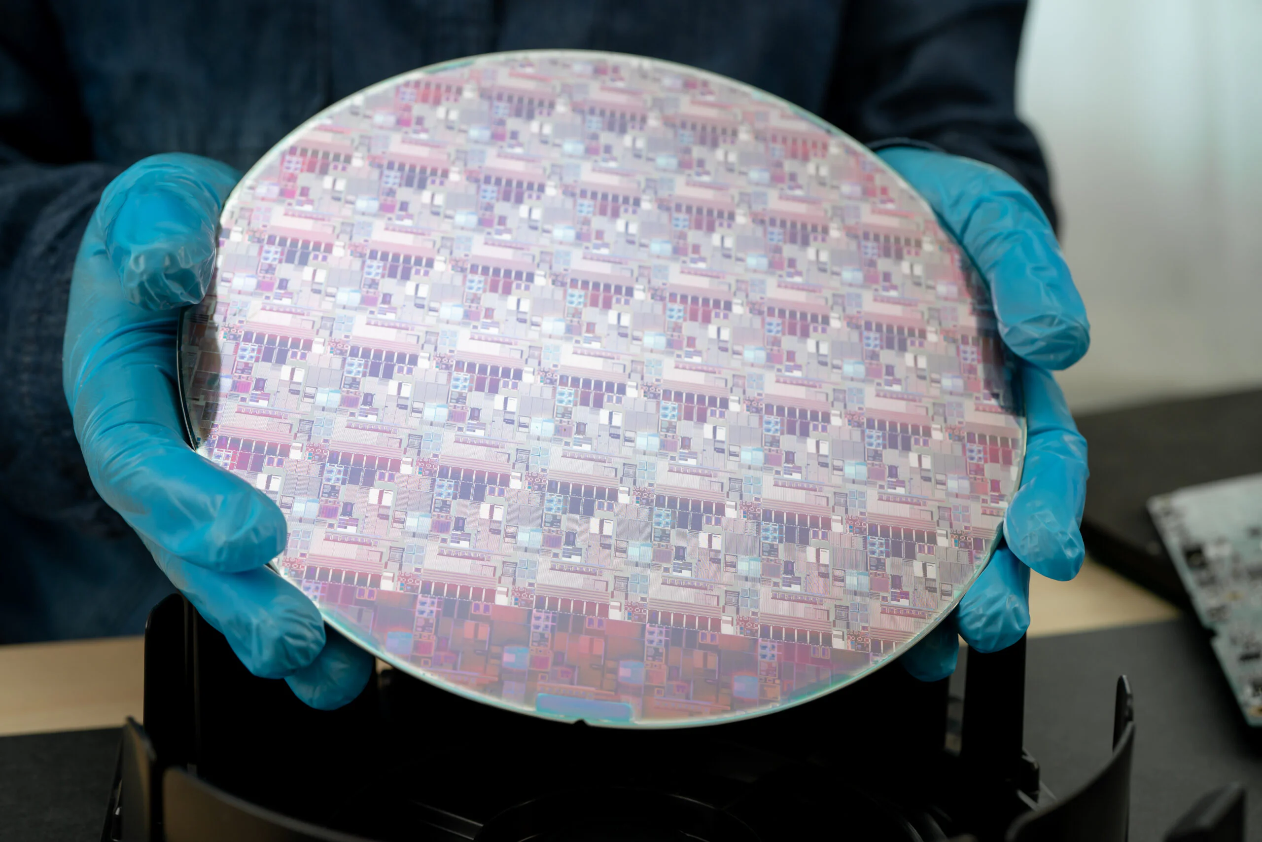
MW-PECVD: Rapid Graphene Growth for Photonic Applications
Astera’s technology is built around a streamlined manufacturing pathway designed to produce photonic-grade graphene with the speed, quality, and scalability needed for real commercial use.
By enabling rapid graphene growth, the process creates a faster path from raw carbon input to a high-performance graphene substrate suitable for photonic applications.
Feedstock Intake
Waste plastics and other carbon inputs are converted into usable source material, creating a scalable starting point for graphene production.
Flash Joule Graphitization
The carbon material is rapidly refined into high-purity graphitic material, forming the quality base needed for advanced photonic applications.
MW-PECVD Deposition
Graphene is grown directly on an engineered substrate, producing a cleaner and more stable semiconductor substrate by avoiding transfer-related defects.
Defect Healing
The material is further refined into photonic-grade monolayer graphene engineered for faster switching, better thermal performance, and greater commercial reliability.
Designed for Real-World Scale
Need a quick answer? Call now.
MARKET OPPORTUNITY
Built at the Intersection of AI, Photonics, and Next-Gen Infrastructure
Astera operates where several powerful trends converge: AI infrastructure expansion, photonic computing adoption, and rising demand for next generation semiconductor materials.
These markets increasingly rely on advanced semiconductor substrate platforms capable of supporting the performance requirements of future computing systems.
Photonic processors
AI data center acceleration
Defense and aerospace systems
Secure communications
Advanced sensing technologies
High-performance optical infrastructure
Astera is building at the foundation of multiple growth markets where next-generation materials can create outsized value.
THE BUSINESS MODEL
Multiple Paths to Commercialization
Direct Revenue Through Substrate Supply
Astera plans to generate revenue by supplying graphene substrates designed for photonic and high-performance computing applications.
- Sale of graphene substrate materials
- Wafer supply supporting advanced graphene photonic chips
- Commercial support for foundry and manufacturing integration
- Participation in the growing demand for next-generation substrate solutions
Scalable Revenue Through Licensing and Partnerships
Astera also has the potential to grow through licensing, joint development, and strategic commercial relationships tied to its technology platform.
- Licensing of proprietary process and substrate technology
- Joint development with photonic device companies and manufacturers
- Strategic partnerships across the photonic ecosystem
- Additional upside through broader platform adoption over time
EARLY ACCESS TO A FOUNDATIONAL LAYER
Why Investors Are Paying Attention
A clear bottleneck in a high-growth market
A differentiated substrate platform designed for photonic computing
Strategic alignment with a photonic ecosystem partner
Multiple commercialization pathways
A vertically integrated IP position
Timing Matters in Platform Technologies
Photonic computing is gaining attention because the need is becoming increasingly clear. AI demand is rising, thermal constraints are intensifying, and conventional materials are approaching their limits.
As this shift accelerates, capital will naturally move toward the companies building the infrastructure behind it. For investors seeking exposure to this opportunity, the most attractive entry point is now.